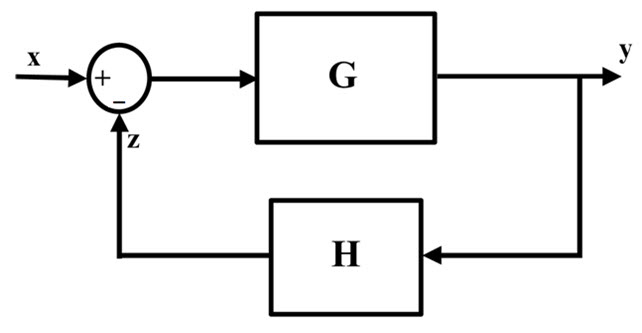
The control systems are classified as 2 types based on the feedback connection, such as closed loop systems and open loop systems. The open loop control systems don’t contain any feedback path where as the closed loop systems contain a feedback path for the automatic correction of errors. Based on the nature of feedback, the closed loop systems are again classified as 2 types, they are Positive feedback systems and Negative feedback systems. In positive feedback systems, the feedback is summed to the input signal. In negative feedback signals, some amount of the signal is subtracted from the input signal to regulate the output. The systems works on the basis of negative systems are known as “negative feedback circuits”. This is also called as “Degenerative feedback”. The basic block diagram of the negative feedback system is shown below with X, Y, Z as input, output and feedback loops respectively.
Transistor feedback circuits
The disadvantage in the circuits designed with transistors is that, the properties like gain, distortion, input and output resistance and the signal to noise ratio depend upon the transistor characteristics. This difficulty can be overcome by introducing the negative feedback. Negative feedback reduces the distortion in the circuit and allows us to control the input and output to the desired level.
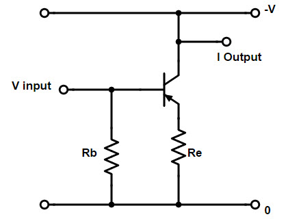
Feedback in emitter follower circuit
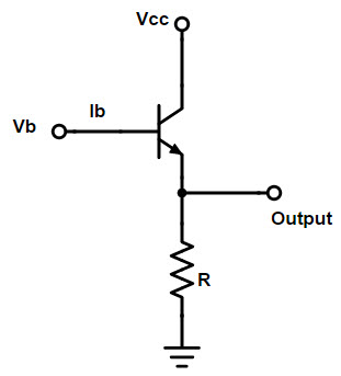
The emitter follower circuit is shown below. The emitter of the transistor is grounded through a resistor and the output is measured at the parallel node of emitter and grounded resistor. Where VBE is the voltage drop between base and emitter of the transistor, the negative feedback operation of the emitter follower circuit can be given as Vin = VBE+Vout.
Now VBE= Vin – Vout. If the feedback quotient of the circuit B = 1, then the gain can be calculated as A = 1/B = 1.
This emitter follower circuit provides two main advantages. They are It provides current amplification without providing any voltage gain It provides impedance matching.
Feedback in common emitter circuit
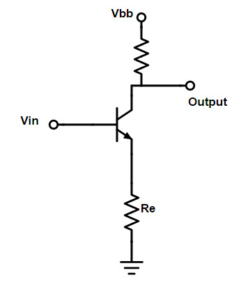
The common emitter circuit is shown below. The emitter of the transistor is grounded through a resistor Re and the output is measured at the parallel node of collector and supply resistor Rc. When the VBE is the voltage drop between base and emitter of the transistor, the input of the common emitter circuit can be given as Vin = VBE + iERE. The output of the circuit is Vout = -ic Rc.
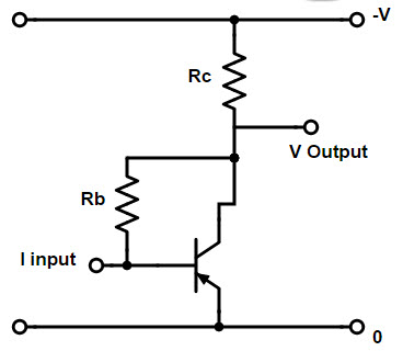
The gain of the circuit is given as Af = – Rc/Re . There are two methods for introducing the negative feedback in common emitter transistors. The two methods are shown below.
The circuits in figure a, b show the same circuit with different method of negative feedback connection.
Op amp feedback circuits
The Op amp circuits connected with feedback are called “op amp feedback circuits”. There are two applications for the op amp with negative feedback connection. They are non inverting op amp circuit inverting op amp circuit.
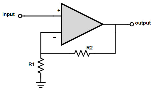
Non inverting op amp circuit
The non inverting op amp circuit is shown below. Input to this circuit is connected to non inverting terminal of the op amp and the feedback signal is connected to the inverting terminal which is grounded with the help of a resistor. So it has high input impedance.
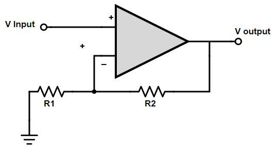
We can easily determine the gain of a non inverting op amp. As the voltage at the both inputs is same, the gain of the op amp will be exceedingly high. Assume that there is no current flow into the op amp, then the current flow in both the resistors is same. As the circuit forms a potential divider circuit the voltage at the inverting input is same as the voltage at the non inverting input that means Vin = Vout x R1 / (R1 + R2). The gain of the non inverting op amp can be calculated as Vout/Vin = AV = 1 + R2/R1 This can be clearly explained by the non inverting amplifier circuit operation. The non inverting amplifier by using an op amp is shown below, in which the input is connected to the positive terminal or the non inverting terminal of the op amp.
In the non inverting amplifier, the nature of output will be same as the nature of input signal. That means, if the input signal is positive, the output also positive similarly, if the input signal is negative, the output also negative. If the open loop gain is AOL, then the output voltage of the non inverting op amp is given as VOut = AOL (Vin – V–) – – – – – – -> (1) Where V- is the function of output voltage, generated because of the voltage divider formed by resistors R1 and R2. As the negative terminal of the op amp will have high impedance, it is equal to V- = β VOut – – – – – – -> (2) Where β = R1 / (R1 + R2). Now substitute the eq (2) in eq (1), we get VOut = AOL (Vin – β VOut) By solving this, we get V¬Out = Vin (1/(β+1/AOL )) If the value of AOL is very high, then substituting the value of β, we get V¬Out = Vin (1+ R1/R2 )
Inverting op amp circuit
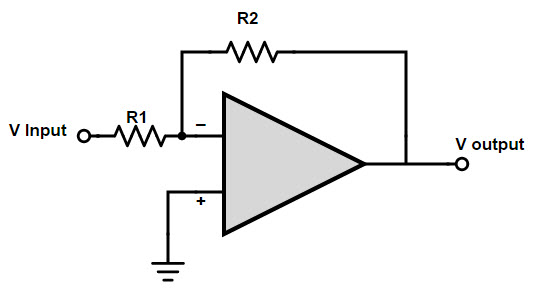
The inverting op amp circuit is shown below. Input to this circuit is connected to inverting terminal or negative terminal of the op amp and the feedback signal is also connected to the inverting terminal. The output of the inverting op amp circuit is 1800 out of phase compared to its input signal and it provides a virtual path.
In this circuit, no current is drawn by the input itself. So the current flow in resistors R1 and R2 is same. Therefore Vout/R2 = Vin/R1. Now the voltage gain of the circuit Av is given as Vout/Vin = AV = – R2/R1 This can be clearly explained by the inverting amplifier circuit operation. The inverting amplifier by using an op amp is shown below, in which the input is connected to the negative terminal or the inverting terminal of the op amp.
In the inverting amplifier, the nature of output will be reverse to the nature of input signal. That means, if the input signal is positive, the output also negative similarly, if the input signal is positive, the output also negative. We can find the gain of the inverting op amp circuit by using the output voltage equation of non-inverting op amp circuit. VOut = AOL (Vin – V–) – – – – – – -> (1) Here V– is calculated by the voltage divider formed by Rf and Rin and it is the function of both input and output voltages (Vout and Vin). So V– = 1/(Rf+ Rin ) (RfVin + Rin Vout) – – – – – – -> (2) Now substitute the eq (2) in eq (1), we get VOut = -Vin . (A(OL ).Rf)/(Rf+ Rin+ A(OL ).Rin) If the value of open loop gain, AOL is very high, then VOut = -Vin (1+ Rf/Rin ) Sometimes, a resistor is inserted between the ground and non inverted output of the op amp, to reduce the input off-set voltage due to the bias current voltage drops. This reduces the distortion in op amps. To eliminate the unwanted DC current, a DC blocking capacitor is connected in series at the input of the op amp.
Advantages of negative feedback
The negative feedback stabilizes almost any type of disturbance or noise occurrence. It is used to overcome the non linearity of the system. It helps us to flatten the frequency response of a system and allows us to get the desired frequency response curve. (decreases frequency distortion) Negative feedback makes the system to less dependent on the temperature and other external properties of the system. It increases the input resistance i.e. it increases input impedance Decreases the output resistance i.e. it decreases output impedance Increases bandwidth of the output signal Decreases the sensitivity of system to the external properties. Provides bias point stability and better CMMR.
Disadvantages of Negative Feedback
The overall gain of the system will be decreased by connecting the negative feedback. If the system is not properly designed, it may lead to produce oscillations.
Comment * Name * Email * Website
Δ





![]()